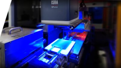
Non-contact crack detection
ISRA’s non-contact inspection system reliably discovers micro-cracks in solar cells without placing the material under mechanical stress.
The patented non-contact imaging technology ensures that the precise detection of micro-cracks is not affected by other material defects. It reliably visualizes and automatically detects even the tiniest cracks, known as “closed cracks,” with minimal overkill.
In contrast to the contacting electroluminescence procedure, the ISRA system avoids any electrical contact with the material as a potential source of new microcracks.
The system is easy to integrate into any production line and allows the reliable identification and removal of damaged cells before further processing or transport.
- Non-contact inspection system for micro-crack detection in solar wafers and cells
- Focusing on microcracks enables the highest detection rates and avoids false defects
- Cumulative defect overlay for identification of systematic faults (handling/processing)
- Image analysis of cumulative defect overlay images
- Applicable for incoming wafer inspection and all following processes like PECVD, Metallization and sorting
- Incoming quality control of full square wafers or half-/triple-cut samples