Wafer production
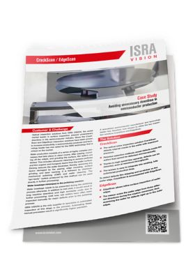
Increase yield while ensuring the highest quality and process reliability, even in ongoing wafer production.
Our inline optical inspection systems reliably detect defects on the surface, at the edge and inside the bulk wafer material to significantly increase your production capacity. Save costs by removing defective material before it reaches the next stage of the production process.
Post-Grinding / Pre-Polishing Inspection
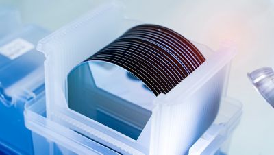
CMP eliminates micro peaks and valleys.
However, microcracks in the bulk wafer material or at the wafer edge can lead to wafer breakage during polishing or other downstream processes, resulting in high costs. Defective wafers must be rejected in time to avoid expensive cleaning and extended machine downtime.
Benefits
- Increased uptime: Microcrack detection minimizes wafer breakage during the polishing process
- Flexibility: Seamless integration into existing process lines
- Efficiency: Simultaneous scanning of bulk and surface at line speeds of up to 180 wafers/hour
- Features
- Typical defects
- Technical data
- Defect detection down to <5 µm crack width
- Wafer mapping / 2D coordination map
- Inspection of the wafer edge from three perspectives
- Scan speed: Up to 130°/sec
- Optional notch inspection
- Chippings
- Micro-cracks
- Etch residuals
- Scratches on the front and rear side
- Crystal defects (twin-lamella)
- High-resolution line scan cameras with LED line illumination using different wavelengths
- Integrated adjustment of thresholds and crack characteristics for sensitive optimization of the detection result
- Typ. resolution: 20 μm, optional down to 1,5 μm
- Optical Setup for edge inspection: 2 × 45° prisms & direct side view for 3-sided image acquired
- Semi standard interface
Download additional information
CrackScan brochure en
- Filename
- brochure-crackscan-semiconductor-en.pdf
- Size
- 311 KB
- Format
EdgeScan brochure en
- Filename
- brochure-edgescan-semiconductor-en.pdf
- Size
- 464 KB
- Format
CrackScan brochure cn
- Filename
- brochure-crackscan-semiconductor-cn.pdf
- Size
- 488 KB
- Format
EdgeScan brochure cn
- Filename
- brochure-edgescan-semiconductor-cn.pdf
- Size
- 523 KB
- Format
Final Quality / End-of-line Inspection
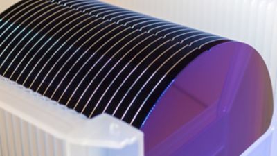
Improve production yields with 100% in-line inspection, even at high inspection speeds. Using patented MultiView technology, our systems reliably identify and classify macro defects, handling scratches or etch residues. This allows defective wafers to be removed from the process at an early stage.
Benefits
- Continuous and complete process control
- Defect detection in a wide range of coating and lamination techniques
- Defects detection on both sides of the web
- Checking of register accuracy
- Features
- Typical defects
- Technical data
- Defect detection on wafer surfaces and wafer edges
- Rear side inspection (non-functional side)
- Front side inspection for GaAs (relaxed requirements)
- Automatic defect classification
- Optional notch inspection
- Scratches on the front and rear side
- Etch pits („round“ polished) on the front side
- Etch defects esp. on the rear side
- Etch residuals
- Edge chippings
- High-resolution line scan cameras
- Highest throughput 50 -100 wph (appl. dep.)
- MultiView technology with adapted wavelength and resolution
- Pixel resolution: typ. 3 μm/px
- Semi standard interface
Download additional information
EdgeScan brochure en
- Filename
- brochure-edgescan-semiconductor-en.pdf
- Size
- 464 KB
- Format
WafQScan brochure en
- Filename
- brochure-wafqscan-semiconductor-en.pdf
- Size
- 233 KB
- Format
EdgeScan brochure cn
- Filename
- brochure-edgescan-semiconductor-cn.pdf
- Size
- 523 KB
- Format
WafQScan brochure cn
- Filename
- brochure-wafqscan-semiconductor-cn.pdf
- Size
- 339 KB
- Format
SpecGAGE3D ensures wafer planarity
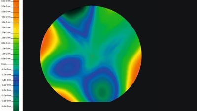
Wafer planarity is essential for perfect assembly. SpecGAGE3D is a compact solution for efficient quality inspection of reflective surfaces. Using deflectometry, height deviations, and defects are reliably detected in a single measurement.
The measurement data is compared to the CAD data, and differences are evaluated within seconds. The system quickly and efficiently determines whether the manufactured wafers are within the required dimensional tolerances. This enables users to minimize production waste while optimizing processes and machine settings.
Integrated into fully automated production lines, SpecGAGE3D permanently improves the process and reduces production costs.
Benefits
- Detects defects on the front and back side of the web
- Reliable checking of register accuracy
- Continuous and seamless process control
- Features
- Typical defects
- Technical data
- Precise height measurement on reflective surfaces for wafer shape inspection
- High detection rate with extremely low slope variations
- Evaluation according to shape and surface defects
- Shape deviations
- Waviness
- Scratches, inclusions, dots
- Measuring principle: Phase measuring deflectometry
- Measuring fields: 300x200 - 600×400 mm²
- Lateral resolution: ~ 20-240 µm
- Accuracy elevation map: +/- 10 μm on 10×10 cm²
Download additional information
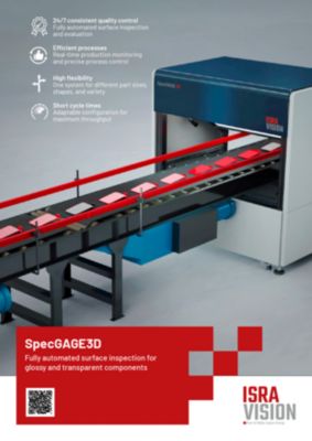
SpecGAGE3D [EN]
- Filename
- mvs-sfa-fl-specgage3d-en-2025-01.pdf
- Size
- 496 KB
- Format
Production analytics - Data-driven efficiency
The web-based production analytics platform allows you to check the system status of all production lines at a glance or analyze production data in detail. With the quality management system, you analyze historical data, monitor current inspection data in real-time, and identify future trends in your production process.
Early detection of production defects
Detect and quickly identify the cause of threshold value violations at every stage of production with live status information and automatic alerts. As a result you can quickly resolve production defects, shorten downtime, and reduce production costs.
Predictive maintenance
You can prevent potential system failures by analyzing real-time data from the sensors and monitoring systems. This allows proactive planning of maintenance, based on the actual condition of the machines, instead of following a fixed schedule. This data-driven approach saves costs through reduced downtime and increased overall productivity, as well as longer production line life.
Optimization of production
Dashboards allow you to compare production line and product data onsite or remotely, providing key insights for optimization. This enables you to make informed professional decisions along your value chain to increase the product quality as well as profitability. You can continuously track the progress of optimization measures and present them with visualized advanced reports.
Your benefits
- Time-saving multi-line overviews, one view for all quality-related information
- Minimize downtime by monitoring system health data
- Faster reaction to quality issues with quality data monitoring
- Fast elimination of production defects, reduction of production costs
- Improved maintenance for reduced downtime, higher overall productivity and longer production line life
Key Features
- Overview on production data and plant status
- Live insights from real time data
- Department oriented dashboards, customer specific adaptations are possible
- Web-based solution, no client software installation required
- Threshold monitoring and alerting
- Open to integrate relevant third-party data and export data to the customer's systems
Service solutions and individual trainings
For the efficient and future-proof operation of your production systems our highly qualified service teams support you globally in all matters. We provide the implementation, maintenance and servicing as well as the analysis and optimization of your systems.
Learn in the ISRA VISION Academy how our competent trainers always keep your employees up to date with the latest knowledge so that system operators, product engineers and quality managers become real inspection experts.


