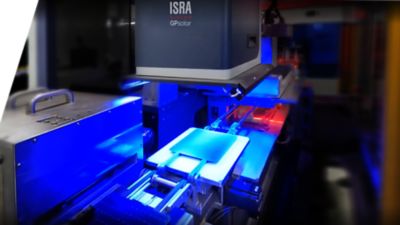
Surface, geometry, and contour inspection in one single measurement unit
Incoming wafer control for full wafer, half-cut wafer and triple-cut wafer: WAF-Q reliably detects visual defects such as fingerprints, stains, surface chippings, and other visible surface defects while also checking dimensional features (edge lengths, angles, chamfer lengths, chamfer angles) and contour defects (intrusions, V-Breaks, Breakage, chamfer breakage).
With its multi-image capturing technology, the system is capable of reliably detecting even low-contrast defects, providing 100% monitoring of wafer production. Based on the data collected, the wafers and cells are then classified into different quality classes.
- Stop-and-Go measurement technology: surface, geometry, and contour inspection
- Wafer sizes from M6 to M12
- Scalable resolutions for highest accuracy requirements from 4MP to 25MP
- Seamless integration into Connected PV for central recipe management and factory defect yield and effect overview