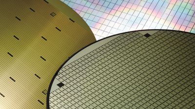
백 엔드 프로세스
무결점 품질의 칩 생산으로 더 높은 수율, 향상된 추적성, 더 빠른 ROI를 달성하세요: 조합 가능한 2D 및 3D 분석 시스템은 모든 칩을 개별적으로 검사하고 집적 회로 패키징을 평가하여 품질 보증을 크게 향상시킵니다. 프론트 엔드와 백엔드 사이의 인터페이스에 통합된 ISRA 검사 시스템은 웨이퍼 레벨과 다이싱 프레임에서 개별 구성 요소의 결함을 감지합니다. 이 100% 검사를 통해 무결점 자재만 고객에게 보내집니다.
웨이퍼 레벨 패키징
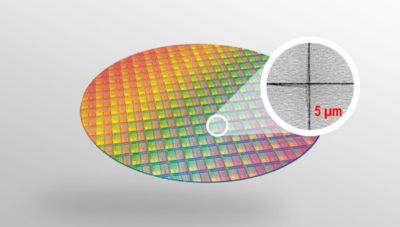
전자 기기의 소형화로 인해 반도체 제조업체는 더 작은 부품 크기를 생산하면서도 더 엄격한 공정 제어 요건을 유지해야 하는 과제를 안고 있습니다.
첨단 웨이퍼 레벨 패키징을 위한 ISRA VISION의 웨이퍼 검사 솔루션은 반도체 제조 공정 전반에 걸쳐 추적성을 보장합니다. 당사의 시스템은 디바이스 성능 향상을 위한 우수한 품질 관리를 제공하여 제조업체가 적시에 공정 편차를 감지, 해결 및 모니터링할 수 있도록 지원합니다.
장점
- 효율성: 벌크 웨이퍼 재료와 웨이퍼 엣지를 동시에 스캔
- 유연성: 기존 프로세스 라인과의 원활한 통합
- 가동 시간 증가: 처리 중 웨이퍼 파손 최소화
- Features
- Typical defects
- Technical data
- 신뢰할 수 있는 결함 감지 및 분류
- 5µm 미만의 균열 폭까지 결함 검출
- 웨이퍼 매핑 / 2D 코디네이션 맵
- 처리량: 최대 180 wph
- Pre-alligner에 통합된 엣지 검사 툴
- 벌크 웨이퍼 재료 내부의 미세 균열
- 엣지 칩핑
- 엣지 근처의 크랙
- 엣지 오염
- 다양한 파장을 사용하는 LED 라인 조명을 갖춘 고해상도 라인 스캔 카메라
- 감지 결과의 민감한 최적화를 위해 임계값 및 크랙 특성을 통합 조정합니다.
- 일반 해상도: 20 μm, 1.5 μm까지 옵션 가능
- 세미 표준 인터페이스
추가 자료 다운로드
 test123
CrackScan brochure en
- Filename
- brochure-crackscan-semiconductor-en.pdf
- Size
- 311 KB
- Format
 test123
CrackScan brochure cn
- Filename
- brochure-crackscan-semiconductor-cn.pdf
- Size
- 488 KB
- Format

EdgeScan brochure en
- Filename
- brochure-edgescan-semiconductor-en.pdf
- Size
- 464 KB
- Format

EdgeScan brochure cn
- Filename
- brochure-edgescan-semiconductor-cn.pdf
- Size
- 523 KB
- Format
박막 (Re-Thinning)

박막(Re-Thinning)은 웨이퍼 표면에 최종 반도체 소자의 성능과 기능에 영향을 줄 수 있는 결함을 유발할 수 있습니다.
따라서 디바이스 기능에 영향을 미칠 수 있는 결함을 감지하기 위해서는 박막화 후 광학 검사가 매우 중요합니다.
박막 재박막 공정 후 광학 검사를 수행하면 제조업체는 결함 위험을 최소화하고 최종 반도체 디바이스가 필요한 성능 및 신뢰성 표준을 충족하도록 보장할 수 있습니다. 이는 반도체 제조 공정의 전반적인 품질과 수율을 향상시키는 데 도움이 됩니다.
장점
- 유연성: 기존 프로세스 라인과의 원활한 통합
- 가동 시간 증가: 처리 중 웨이퍼 파손 최소화
- 효율성: 시간당 최대 180 웨이퍼의 라인 속도로 벌크와 표면을 동시에 스캔
- 웨이퍼 처리 솔루션에 맞춤형으로 원활하게 통합
- 다른 공정 단계와 병행하여 재박막 웨이퍼 엣지를 100% 제어 - 기존 사이클 타임에 영향 없음
- Features
- Typical defects
- Technical data
- 신뢰할 수 있는 결함 감지 및 분류
- 5µm 미만의 균열 폭까지 결함 검출
- 웨이퍼 매핑 / 2D 코디네이션 맵
- 다시 얇아진 웨이퍼 가장자리에서 크랙/칩아웃의 공정 제어
- 처리량: 최대 180 wph
- Pre-aligner에 통합된 에지 검사 툴
- 벌크 웨이퍼 재료 내부의 미세 크랙
- 엣지 칩핑
- 엣지 근처의 크랙
- 오염
- 다양한 파장을 사용하는 LED 라인 조명을 갖춘 고해상도 라인 스캔 카메라
- 검출 결과의 민감한 최적화를 위한 임계값 및 균열 특성 통합 조정
- 미세 균열 검사를 위한 일반적인 해상도: 20 μm, 옵션으로 1.5 μm까지 가능
- 엣지 검사를 위한 픽셀 해상도: 통상 3μm/px
- 얇은 웨이퍼 처리와 통합
- 세미 표준 인터페이스
추가 자료 다운로드

CrackScan brochure en
- Filename
- brochure-crackscan-semiconductor-en.pdf
- Size
- 311 KB
- Format
test123
CrackScan brochure cn
- Filename
- brochure-crackscan-semiconductor-cn.pdf
- Size
- 488 KB
- Format
EdgeScan brochure en
- Filename
- brochure-edgescan-semiconductor-en.pdf
- Size
- 464 KB
- Format
EdgeScan brochure cn
- Filename
- brochure-edgescan-semiconductor-cn.pdf
- Size
- 523 KB
- Format
다이싱 후 검사 반도체 제조에서 다이싱 스트리트의 100% 검사
웨이퍼 다이싱은 다이싱 스트리트에 결함이 발생할 위험이 있습니다. 다이싱 스트리트를 정확하게 검사하면 이러한 결함을 확실하게 감지하고 칩과 다이의 불량률을 최소화할 수 있습니다. DicingScan 검사 툴은 100% 웨이퍼 검사를 제공합니다. 고성능 라인 스캔 카메라는 다이싱 스트리트의 엣지 칩핑과 같은 결함을 정밀하게 감지합니다. 또한 이 툴은 다이싱 스트리트의 존재 여부, 위치, 완전성을 검사합니다.
특허를 받은 멀티뷰 이미징 기술은 WafQScan 공정의 기반이 되며, 사용자는 캐리어 테이프(포일)를 통해 웨이퍼의 뒷면도 검사할 수 있습니다. 다이싱스캔은 완벽한 품질의 다이/칩만 처리할 수 있도록 보장합니다.
장점
- 효율성: 한 번의 스캔으로 여러 검사 작업 수행
- 100% 품질 관리: 고품질 금형과 칩만 가공
- Features
- Typical defects
- Technical data
- 다이싱 직후 다이싱 스트리트 검사
- 다이스의 (미세) 크랙 검사
- 다이싱 스트리트의 위치, 무결성 및 품질 검사
- 캐리어 테이프를 통해서도 전면 및 후면 검사
- Uncompleted dicing
- Cracks
- Bubbles
- Releases
- Chip-outs
- 동시 이미지 캡처가 가능한 멀티뷰 기술
- 준표준 인터페이스
생산 분석 - 데이터 기반 생산 효율성
웹 기반 생산 분석 플랫폼을 통해 모든 생산 라인의 시스템 상태를 한눈에 확인하거나 생산 데이터를 세부적으로 분석할 수 있습니다. 품질 관리 시스템을 통해 과거 데이터를 분석하고, 현재 검사 데이터를 실시간으로 모니터링하며, 생산 공정의 향후 추세를 파악할 수 있습니다.
생산 최적화
대시보드를 통해 생산 라인과 제품 데이터를 현장 또는 원격으로 비교하여 최적화를 위한 핵심 인사이트를 얻을 수 있습니다. 이를 통해 가치 사슬 전반에 걸쳐 정보에 입각한 전문적인 의사 결정을 내릴 수 있어 제품 품질과 수익성을 높일 수 있습니다. 최적화 조치의 진행 상황을 지속적으로 추적하고 시각화된 고급 리포트를 통해 이를 제시할 수 있습니다
생산 결함 조기 발견
실시간 상태 정보와 자동 알림을 통해 생산의 모든 단계에서 임계값 위반의 원인을 감지하고 신속하게 파악할 수 있습니다. 그 결과 생산 결함을 신속하게 해결하고 가동 중단 시간을 단축하며 생산 비용을 절감할 수 있습니다.
예측 유지보수
센서와 모니터링 시스템의 실시간 데이터를 분석하여 잠재적인 시스템 장애를 예방할 수 있습니다. 이를 통해 정해진 일정에 따르지 않고 기계의 실제 상태를 기반으로 유지보수를 사전에 계획할 수 있습니다. 이러한 데이터 기반 접근 방식은 다운타임을 줄이고 전반적인 생산성을 높임으로써 비용을 절감할 뿐만 아니라 생산 라인 수명을 연장합니다.
이점
- 시간을 절약하 수 있는 multi-line overview, 모든 품질 관련 정보를 한 번에 볼 수 있는 One view 시스템
- 시스템 상태 데이터 모니터링으로 다운타임 최소화
- 품질 데이터 모니터링으로 품질 문제에 대한 신속한 대응
- 생산 결함의 신속한 제거, 생산 비용 절감
- 유지보수 개선으로 다운타임 감소, 전체 생산성 향상 및 생산 라인 수명 연장
특징
- 생산 데이터 및 공장 상태에 대한 Overview
- 실시간 데이터에서 얻은 Live 로 인사이트 확보
- 웹 기반 솔루션 (클라이언트 소프트웨어 설치 필요 없음)
- 임계값 모니터링 및 경고
- 사업부 중심의 대시보드, 고객별 맞춤 설정 가능
- 관련 타사 데이터 통합 가능 및 고객 시스템으로 데이터 내보내기 가능
맞춤형 서비스 솔루션 및 개별 교육


생산 시스템의 효율적이고 미래 지향적인 운영을 위해 우수한 자격을 갖춘 서비스팀이 모든 문제에 대해 전 세계적으로 고객을 지원합니다. 연중무휴 24시간 신속하고 안정적으로 시스템의 구현, 유지보수 및 서비스는 물론 분석 및 최적화를 제공합니다.
또한 유능한 트레이너를 통해 시스템 운영자, 제품 엔지니어 및 품질 관리자가 진정한 검사 전문가가 될 수 있도록 직원들에게 항상 최신 지식을 제공하는 방법을 알아보시려면 ISRA 아카데미를 방문하세요.