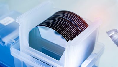
Wafer production
Increase yield while ensuring the highest quality and process reliability, even in ongoing wafer production.
Our inline optical inspection systems reliably detect defects on the surface, at the edge and inside the bulk wafer material to significantly increase your production capacity. Save costs by removing defective material before it reaches the next stage of the production process.
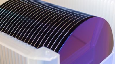
Post-Grinding / Pre-Polishing Inspection
CMP eliminates micro peaks and valleys.
However, microcracks in the bulk wafer material or at the wafer edge can lead to wafer breakage during polishing or other downstream processes, resulting in high costs. Defective wafers must be rejected in time to avoid expensive cleaning and extended machine downtime.
Benefits
- Increased uptime: Microcrack detection minimizes wafer breakage during the polishing process
- Flexibility: Seamless integration into existing process lines
- Efficiency: Simultaneous scanning of bulk and surface at line speeds of up to 180 wafers/hour
- Features
- Typical defects
- Technical data
- Defect detection down to <5 µm crack width
- Wafer mapping / 2D coordination map
- Inspection of the wafer edge from three perspectives
- Scan speed: Up to 130°/sec
- Optional notch inspection
- Chippings
- Micro-cracks
- Etch residuals
- Scratches on the front and rear side
- Crystal defects (twin-lamella)
- High-resolution line scan cameras with LED line illumination using different wavelengths
- Integrated adjustment of thresholds and crack characteristics for sensitive optimization of the detection result
- Typ. resolution: 20 μm, optional down to 1,5 μm
- Optical Setup for edge inspection: 2 × 45° prisms & direct side view for 3-sided image acquired
- Semi standard interface
Download additional information
 asdf
asdf
CrackScan brochure en
- Filename
- brochure-crackscan-semiconductor-en.pdf
- Size
- 311 KB
- Format
 test123
EdgeScan brochure en
- Filename
- brochure-edgescan-semiconductor-en.pdf
- Size
- 464 KB
- Format

CrackScan brochure cn
- Filename
- brochure-crackscan-semiconductor-cn.pdf
- Size
- 488 KB
- Format

EdgeScan brochure cn
- Filename
- brochure-edgescan-semiconductor-cn.pdf
- Size
- 523 KB
- Format
Final Quality / End-of-line Inspection
Improve production yields with 100% in-line inspection, even at high inspection speeds. Using patented MultiView technology, our systems reliably identify and classify macro defects, handling scratches or etch residues. This allows defective wafers to be removed from the process at an early stage.
Benefits
- Continuous and complete process control
- Defect detection in a wide range of coating and lamination techniques
- Defects detection on both sides of the web
- Checking of register accuracy
- Features
- Typical defects
- Technical data
- Defect detection on wafer surfaces and wafer edges
- Rear side inspection (non-functional side)
- Front side inspection for GaAs (relaxed requirements)
- Automatic defect classification
- Optional notch inspection
- Scratches on the front and rear side
- Etch pits („round“ polished) on the front side
- Etch defects esp. on the rear side
- Etch residuals
- Edge chippings
- High-resolution line scan cameras
- Highest throughput 50 -100 wph (appl. dep.)
- MultiView technology with adapted wavelength and resolution
- Pixel resolution: typ. 3 μm/px
- Semi standard interface
Download additional information
EdgeScan brochure en
- Filename
- brochure-edgescan-semiconductor-en.pdf
- Size
- 464 KB
- Format

WafQScan brochure en
- Filename
- brochure-wafqscan-semiconductor-en.pdf
- Size
- 233 KB
- Format
EdgeScan brochure cn
- Filename
- brochure-edgescan-semiconductor-cn.pdf
- Size
- 523 KB
- Format

WafQScan brochure cn
- Filename
- brochure-wafqscan-semiconductor-cn.pdf
- Size
- 339 KB
- Format
SpecGAGE3D ensures wafer planarity
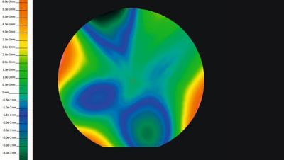
Wafer planarity is essential for perfect assembly. SpecGAGE3D is a compact solution for efficient quality inspection of reflective surfaces. Using deflectometry, height deviations, and defects are reliably detected in a single measurement.
The measurement data is compared to the CAD data, and differences are evaluated within seconds. The system quickly and efficiently determines whether the manufactured wafers are within the required dimensional tolerances. This enables users to minimize production waste while optimizing processes and machine settings.
Integrated into fully automated production lines, SpecGAGE3D permanently improves the process and reduces production costs.
Benefits
- Detects defects on the front and back side of the web
- Reliable checking of register accuracy
- Continuous and seamless process control
- Features
- Typical defects
- Technical data
- Precise height measurement on reflective surfaces for wafer shape inspection
- High detection rate with extremely low slope variations
- Evaluation according to shape and surface defects
- Shape deviations
- Waviness
- Scratches, inclusions, dots
- Measuring principle: Phase measuring deflectometry
- Measuring fields: 300x200 - 600×400 mm²
- Lateral resolution: ~ 20-240 µm
- Accuracy elevation map: +/- 10 μm on 10×10 cm²
Download additional information
생산 분석 - 데이터 기반 생산 효율성
웹 기반 생산 분석 플랫폼을 통해 모든 생산 라인의 시스템 상태를 한눈에 확인하거나 생산 데이터를 세부적으로 분석할 수 있습니다. 품질 관리 시스템을 통해 과거 데이터를 분석하고, 현재 검사 데이터를 실시간으로 모니터링하며, 생산 공정의 향후 추세를 파악할 수 있습니다.
생산 최적화
대시보드를 통해 생산 라인과 제품 데이터를 현장 또는 원격으로 비교하여 최적화를 위한 핵심 인사이트를 얻을 수 있습니다. 이를 통해 가치 사슬 전반에 걸쳐 정보에 입각한 전문적인 의사 결정을 내릴 수 있어 제품 품질과 수익성을 높일 수 있습니다. 최적화 조치의 진행 상황을 지속적으로 추적하고 시각화된 고급 리포트를 통해 이를 제시할 수 있습니다
생산 결함 조기 발견
실시간 상태 정보와 자동 알림을 통해 생산의 모든 단계에서 임계값 위반의 원인을 감지하고 신속하게 파악할 수 있습니다. 그 결과 생산 결함을 신속하게 해결하고 가동 중단 시간을 단축하며 생산 비용을 절감할 수 있습니다.
예측 유지보수
센서와 모니터링 시스템의 실시간 데이터를 분석하여 잠재적인 시스템 장애를 예방할 수 있습니다. 이를 통해 정해진 일정에 따르지 않고 기계의 실제 상태를 기반으로 유지보수를 사전에 계획할 수 있습니다. 이러한 데이터 기반 접근 방식은 다운타임을 줄이고 전반적인 생산성을 높임으로써 비용을 절감할 뿐만 아니라 생산 라인 수명을 연장합니다.
이점
- 시간을 절약하 수 있는 multi-line overview, 모든 품질 관련 정보를 한 번에 볼 수 있는 One view 시스템
- 시스템 상태 데이터 모니터링으로 다운타임 최소화
- 품질 데이터 모니터링으로 품질 문제에 대한 신속한 대응
- 생산 결함의 신속한 제거, 생산 비용 절감
- 유지보수 개선으로 다운타임 감소, 전체 생산성 향상 및 생산 라인 수명 연장
특징
- 생산 데이터 및 공장 상태에 대한 Overview
- 실시간 데이터에서 얻은 Live 로 인사이트 확보
- 웹 기반 솔루션 (클라이언트 소프트웨어 설치 필요 없음)
- 임계값 모니터링 및 경고
- 사업부 중심의 대시보드, 고객별 맞춤 설정 가능
- 관련 타사 데이터 통합 가능 및 고객 시스템으로 데이터 내보내기 가능
맞춤형 서비스 솔루션 및 개별 교육


생산 시스템의 효율적이고 미래 지향적인 운영을 위해 우수한 자격을 갖춘 서비스팀이 모든 문제에 대해 전 세계적으로 고객을 지원합니다. 연중무휴 24시간 신속하고 안정적으로 시스템의 구현, 유지보수 및 서비스는 물론 분석 및 최적화를 제공합니다.
또한 유능한 트레이너를 통해 시스템 운영자, 제품 엔지니어 및 품질 관리자가 진정한 검사 전문가가 될 수 있도록 직원들에게 항상 최신 지식을 제공하는 방법을 알아보시려면 ISRA 아카데미를 방문하세요.