Optical inspection system identifies and locates smallest cracks inside bulk wafer material
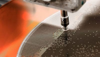
100% inspection of dicing streets in semiconductor manufacturing
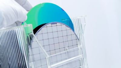
100% wafer edge inspection and reliable defect detection
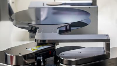
Automatic surface inspection of highly reflective objects
Reliable detection of defects, such as contaminations or micro scratches