Excellent defect detection on semiconductor wafer surfaces
WafQScan enables 100% inline surface inspection of semiconductor wafers. Using pixel-synchronous images captured under different illumination scenarios, the patented MultiView technology ensures excellent defect detection rates in a single scan. WafQScan is the ideal solution for applications for bare, cut and processed wafers.
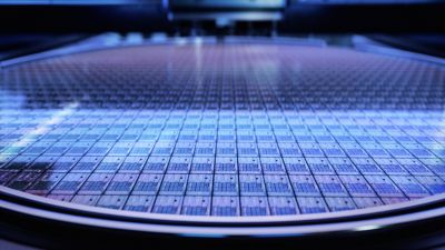
Defect detection on wafer surfaces with WafQScan
The system reliably detects all defects, such as contaminations and etching residues. By identifying defects early on and ejecting defective wafers, WafQScan ensures maximum yield and optimum capacity utilization. Users thus benefit from a quick return on investment.
Complementing the system with the EdgeScan option, users can conduct optical inspection of the wafer edge, in addition to the surface inspection.
- MultiView-technology with adapted wavelength and resolution
- Manual or fully automated configurations
- Inspection module with SEMI hard- and software interface
Download additional information
 Automotive Overview brochure
WafQScan brochure en
- Filename
- brochure-wafqscan-semiconductor-en.pdf
- Größe
- 233 KB
- Format

WafQScan brochure cn
- Filename
- brochure-wafqscan-semiconductor-cn.pdf
- Größe
- 339 KB
- Format