- INSPECTION SOLUTIONS FOR SOLAR WAFERS & CELLS
- Wafer and cell manufacturing
- Geometry & Contour Inspection
- Microcrack Inspection
- Surface Inspection
- Texturing Inspection
- Pre- and Post-Coating PL Inspection
- Color & Coating Inspection
- Photoluminescence (PL) Inspection
- Print Inspection
- Plating Inspection
- Pattern & Structure Inspection
- Final Inspection & Classification
- Data Analytics / CPV
- Servicelösungen und Schulungen
- Kontakt aufnehmen
Wafer and cell manufacturing
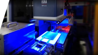
The ideal system for every process step – Solar cell inspection solutions from ISRA VISION / GP Solar
The demand for ever more powerful cells is growing at an almost unstoppable rate. At the same time, manufacturers need the best quality with maximum throughput to be able to produce economically.
With our unique inspection portfolio, we ensure meeting all quality requirements while envisioning full production transparency not only at the system or line level, but also across entire sites. You benefit from maximum efficiency, flexibility, and cost-effectiveness.
Geometry & Contour Inspection
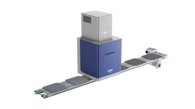
Detect edge distortions and geometric irregularities in less than one second cycle times. Our inspection systems sort the inspected wafers into different quality classes based on their geometric properties. Wafers that do not meet the desired quality can thus be removed before further processing – ensuring high quality for excellent module effectiveness and permanently reduced warranty costs.
The "Copy-Exact" calibration concept lets users quickly transfer inspection recipes and settings between production lines. This ensures a uniform inspection standard and reduces the system set-up workload.
Benefits
- Save process resources - reject bad wafers at the start
- Proceed only good wafers from the start to enable the best cell efficiency at the end
- Features
- Typical defects
- Technical data
- Incoming quality control of full square wafers or half-cut samples
- Check for any breakage or damage to the outer contour
- Use of matrix cameras to ensure perfect reliability of measured dimensional accuracy
- Efficient: Evaluate two or more half cells with only one image acquisition
- Precise metrological calibration traceable to national standards
- Seamless integration into Connected PV for central recipe management and factory defect yield and effect overview
- Dimensional defects: non-rectangularity (angles <>90°), size mismatch (edge lengths <> specified value), chamfer length deviations
- Contour defects: intrusions, V-breaks, breakage, chippings
- Solutions for on-the-fly measurement and stop-and-go automation
- On the fly, checks only geometry and contour
- Stop & Go, combined with surface inspection
- On the fly, edge chippings, combined with micro-crack
Download additional information

Solar cell inspection portfolio
- Filename
- mvs-so-pv-cell-overview.en1.pdf
- Größe
- 5 MB
- Format
Microcrack Inspection
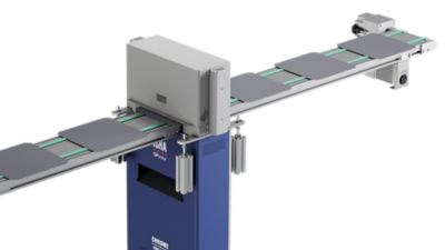
Microcracks in wafers or cells can cause breakage during downstream processes or in the finished module. This can result in reduced production throughput or degraded performance in the field. Non-contact crack detection technology identifies affected wafers and cells without mechanically stressing the material. Immediate ejection lowers processing costs and boosts resource-efficient production.
Benefits
- Increase production throughput - eliminate downtime caused by broken silicon wafers
- Save resources – use material and machines to process only wafers that do not break
- Improve your processes: identify (handling) equipment that introduces cracks, and fix them to reduce line breakage
- Reclaim wafers with microcracks – improve manufacturing and wafer handling processes for wafer suppliers
- Features
- Typical defects
- Technical data
- Incoming quality control of full square wafers or half-/triple-cut samples
- Check for microcracks at any process step (not possible with full area metal, no inspection at metal-covered positions (e.g., below busbars/finger grid)
- Unique illumination technology to make the smallest microcracks visible
- Very sensitive to small edge chippings as they occur due to combined laser/mechanical separation of half- and triple-cut wafers
- Microcracks
- Contour Defects: intrusions, V-breaks, breakage, chippings
- NANO-D for on-the-fly crack detection
Download additional information

Solar cell inspection portfolio
- Filename
- mvs-so-pv-cell-overview.en1.pdf
- Größe
- 5 MB
- Format
Surface Inspection

Innovative inspection technology reliably and repeatedly detects visual defects such as stains, fingerprints, or chips on the surface of as-cut wafers. With its multi-image capture technology, the system can reliably detect even low-contrast defects, enabling 100% monitoring of wafer production. It classifies the wafers into different quality classes based on the data collected.
Line-scan camera technology allows on-the-fly inspection with a moving sample, enabling the highest throughput.
Benefits
- Save resources – use material and machines to process only good wafers
- Increase efficiency and identify process weaknesses early: modify (handling) equipment that causes contaminations or damages
- Features
- Typical defects
- Technical data
- Incoming quality control of full square wafers or half-/triple-cut samples
- Inspection of the wafer surface for even low-contrast visual defects and visible contamination and damage
- Reporting of the count, size, and position for each defect type
- Stains, fingerprints, dust particles, scratches, watermarks, and other visible surface defects
- WAF-Q: Stop & Go, surface inspection combined with contour check and precise dimensional check
- WAF-Q SCAN: on-the-fly, surface and contour inspection only
Download additional information

Solar cell inspection portfolio
- Filename
- mvs-so-pv-cell-overview.en1.pdf
- Größe
- 5 MB
- Format
Texturing Inspection
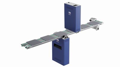
Texture strongly influences the color appearance and the efficiency of the finished cell. Defective and insufficiently textured wafers that are overlooked here take up valuable machine resources in the subsequent process steps.
The TEX-Q inspection system precisely monitors the cell surface for contamination and defects while checking the texturing for homogeneity and reflectivity. The cameras can also be fitted beneath the roller transport.
Benefits
- Save resources: identify texturing problems early in the line
- Quickly counteract any process deviations
- Remove bad cells early in time, avoid cost-intensive further processing
- Features
- Typical defects
- Technical data
- Texturing quality monitoring: Inspection of homogeneity and reflectivity
- Check for contaminations and defects, long-term drifts
- Connected PV "boat view": trace back faulty cells to carrier, machine, and chemical bath
- Cycle times <0.7 sec for the highest throughputs
- Line scan technology for the highest sensitivity
- Flow marks ("comets")
- Dark spots
- Flow patterns
- Contaminations
- Texture inhomogeneity
- Line scan camera technology for easy integration into on-the-fly processes
- Suitable for every texture: alkaline, acidic, MCCE (black silicon)
- Inspection of wafer sizes from M6 to M12+
Download additional information

Solar cell inspection portfolio
- Filename
- mvs-so-pv-cell-overview.en1.pdf
- Größe
- 5 MB
- Format
Pre- and Post-Coating PL Inspection

Material properties play a critical role in cell efficiency. Photoluminescence can be used to verify the electrical properties of materials within a cell. The LUMI-Q Coating system is specifically designed for pre- and post-coating photoluminescence inspection. It automatically detects defects that affect cell efficiency, allowing users to optimize processes and eliminate defective material in a timely manner.
Benefits
- Increased process yield & uptime: Immediate process feedback, correction of machine failures and deviations
- Quality: Support raising the cell efficiency
- Easy integration: Small footprint, no additional handling, no additional cycle time
- Full support for Connected PV data analysis
- Features
- Typical defects
- Technical data
- Photoluminescence inspection for pre- and post-coating
- Laser-free – reduced safety requirements
- Seamless integration into standard handling equipment
- On-the-fly scanning
- Seamless integration into GP Software Suite and Fab Data management (CPV)
- Central recipe management
- Central data reporting
- Interface MES system
- Material defects: Microcracks, impurities, crystal defects
- Coating defects: Scratches, stains, passivation defects
- Fast measurement speed: ≥ 1500 mm/s @ 1k
Download additional information

LUMI-Q Coating
- Filename
- mvs-so-fl-lumi-q-coating-en-2024-07.pdf
- Größe
- 3 MB
- Format
Color & Coating Inspection
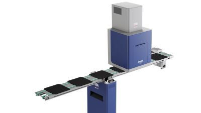
Homogeneous color and coating are a prerequisite for homogeneous modules.
Color and defect inspection with COL-Q immediately after the coating process ensures fast intervention in the case of color deviations. CELL-Q checks the color and coating quality during the final inspection and sorts the cells into different performance classes based on their optical properties.
Benefits
- Improve efficiency and quality: Achieve direct process feedback and act on process deviations
- Examine the possibility of reworking to improve yield
- Save print paste metallization cost by sorting out defective cells in time
- Accelerate your ramp-up with Connected PV
- Features
- Typical defects
- Technical data
- Inspection of color (HSV color model based on RGB color measurement)
- Inspection of coating thickness (use a physical model to calculate a layer thickness)
- PRO Matrix systems: full camera resolution at 2 Bit color depth - no interpolation
- Detection of inhomogeneous samples
- Inspection of the bottom side with the line-scan system without flipping
- ConnectedPV "Boat View": trace back defective samples to the individual boat/furnace/tube/position in the process
Coating defects, inhomogeneities, wrong coating thickness
- On-the-fly inspection with up to 1,500 mm/s (resolution 2k), up to 2,000 mm/s (1k)
- Unrivaled color repeatability of < 0.5 deg (H), <0.5 % (S,V)
Download additional information

Solar cell inspection portfolio
- Filename
- mvs-so-pv-cell-overview.en1.pdf
- Größe
- 5 MB
- Format
Photoluminescence (PL) Inspection
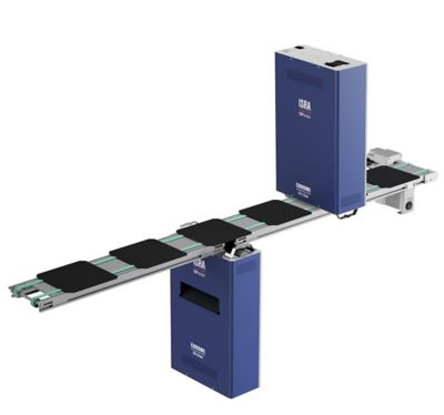
Printing solar cells is one of the most expensive process steps in the cell production chain. Therefore, detecting process deviations at an early stage is crucial.
Discover the market-leading print pattern monitoring and inspect reliably at the highest line speeds. Identify and classify low-micron discontinuities and deliver cells of the highest quality.
Benefits
- Check the rework possibility to improve yield
- Increase efficiency and quality: Achieve direct process feedback and take countermeasures on process deviations
- Fast process ramp-up with Connected PV
- Save production resources and print paste metallization cost by sorting out before metallization
- Features
- Typical defects
- Technical data
- Laser-free technology (patent pending)
- No laser safety – low safety measures
- Different excitation wavelengths available for specific applications
- Inspection of diffusion homogeneity, surface passivation, contamination, and metallization defects
All defects that cause carrier losses that reduce the radiative recombination (which generates the luminescence)
- Microcracks and breakage
- Surface passivation problems
- Impurities and contamination
- Shunts and series resistance variations
- On-the-fly inspection
- 500 mm/s @ 3k TDI
- 900 mm/s @ 1k TDI
- 1500 mm @ 1k InGaAs
- < 0.6 sec cycle time
Download additional information

Solar cell inspection portfolio
- Filename
- mvs-so-pv-cell-overview.en1.pdf
- Größe
- 5 MB
- Format
Print Inspection
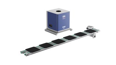
Printing solar cells is one of the most expensive process steps in the cell production chain. Therefore, detecting process deviations at an early stage is crucial.
Discover the market-leading print pattern monitoring and inspect reliably at the highest line speeds. Identify and classify low-micron discontinuities and deliver cells of the highest quality.
Benefits
- Small footprint - integration on rotary table possible
- Shortest ramp-up times with Connected PV
- Immediate detection of print defects, which sometimes are only cosmetic, but can lead to loss of efficiency
- Features
- Typical defects
- Technical data
- Inspection of each printing step directly on a rotary table or immediately following the print table unloading
- Inspection of the print pattern features based on a CAD-like model of the print pattern
- Detection and quantification of deviations from the expected print pattern design
- Higher accuracy than pattern matching from a teched pattern
- Print alignment control - check that the print is correctly aligned with other structures on the cell (laser contact openings, selective emitter structures, and others)
- Fast breakage signal in case of wafer breakage to avoid consequential misprinting
- Feedback of print position, busbar position, and other information to automation for use as feedback loop input for automatic print adjustment or positioning of IV tester contact bars in final sorting
- Finger interrupts, thinnings, slubs, nodes, paste stains, and smearings, missing paste on busbar
- Measurement of local finger-width, incl. probe regions, for comparison with offline data
- Measurement of print position and misalignment with other structures
- Special set of defects for IBC cell print patterns (bridging and others)
- < 0.7 sec cycle time for a single image (print and fiducials only) in PRINT-Q
- < 0.6 sec cycle time for a single image (print and fiducials) in PRINT-Q SCAN
Download additional information

Solar cell inspection portfolio
- Filename
- mvs-so-pv-cell-overview.en1.pdf
- Größe
- 5 MB
- Format
Plating Inspection

Flawless plating improves conductivity and increases the efficiency of the solar cell. Careful quality control and monitoring are essential to ensure solar cells are uniformly plated. Manufacturers must quickly identify inhomogeneities, surface adhesion problems, and contaminations before affecting quality. This ensures high durability and prevents efficiency loss.
Benefits
- Immediate detection of plating defects, which sometimes are simply cosmetic, but can lead to severe efficiency loss
- Shortest ramp-up times and easy-to-implement global quality settings with Connected PV
- Features
- Typical defects
- Technical data
- After plating inspection of the contact pattern features, based on a CAD-like model of the pattern
- Higher accuracy than pattern matching from a teched pattern
- Detection of typical plating defects like ghost-plating and detached fingers
- Measurement of contact grid position
- Detection and quantification of deviations from the expected pattern design
- Contact grid quality inspection with all of the above also in the final sorting
- Finger interrupts, thinnings, slubs, nodes, stains, ghost plating, missing plating
- Measurement of local finger-width, incl. probe regions, for comparison with offline data
- Measurement of print position and misalignment with other structures
- < 0.7 sec cycle time for a single image (grid and fiducials only) in PRINT-Q
- < 0.6 sec cycle time for a single image (grid and fiducials) in PRINT-Q SCAN
Download additional information

Solar cell inspection portfolio
- Filename
- mvs-so-pv-cell-overview.en1.pdf
- Größe
- 5 MB
- Format
Pattern & Structure Inspection

For high-performance cells such as IBCs (Interdigitated Back Contact), the perfect alignment of the individual layers is a prerequisite for realizing the full cell performance potential.
Even the slightest shift in the pattern or structure will result in a loss of cell efficiency.
Our inspection solutions for patterns and structures not only detect optical defects such as finger breaks but also check the correct alignment and position of the different layers in relation to each other.
Benefits
- Instant process feedback to quickly identify and correct process weaknesses
- Shortest ramp-up times and easy-to-implement global quality settings with Connected PV
- Features
- Typical defects
- Technical data
- Controlling the pattern accuracy of structured layers directly after structuring: detect deviations from the desired form and the desired position of the pattern
- Inspection of pattern features based on a CAD-like model of the pattern, or special "no teaching" algorithms
- Inspect patterned layers, e.g., for IBC cell fabrication: printed, plasma or chemically deposited, laser structured, shadow mask evaporated, or any other type of patterned layer
- Obtain information on the color, thickness, and optical quality of the layer
- Interrupts, thinnings, nodes, slubs, bridgings, holes, misalignment of the pattern
- Thickness deviation, color deviation of the layer
- Positioning of the pattern on the wafer relative to underlying structures
- On-the-fly or stop-and-go measurement is possible, depending on layer, pattern, and application
Solutions:
- PRINT-Q SE for simple pattern inspection
- PRINT-Q SCAN for simple pattern inspection on-the-fly
- PRINT-Q SBD for pattern, layer, and full-area alignment control
- CELL-Q for final sorting
Download additional information

Solar cell inspection portfolio
- Filename
- mvs-so-pv-cell-overview.en1.pdf
- Größe
- 5 MB
- Format
Final Inspection & Classification
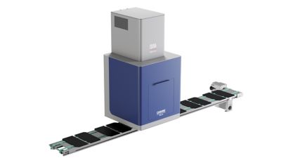
Cell sorting at the end of the line is mandatory for high-value modules of homogenous color.
The CELL-Q inline inspection system checks the front or back of solar cells and sorts them into different color and quality classes according to their optical properties. In a single inspection step, CELL-Q checks every solar cell's print quality and anti-reflection coating.
Any print and color defects on all cell technologies are reliably detected. Additionally, CELL-Q identifies visible surface and contour defects to ensure that only homogeneous cells regarding color and performance are processed within one module.
Benefits
- Proven and reliable calibration concept
- Equal performance across lines with a single central recipe
- Shortest ramp-up times and easy-to-implement global quality settings with Connected PV
- Features
- Typical defects
- Technical data
- Sorting of cells in color classes
- Sorting of cells according to the optical quality of the contact grid
- Separate result classes for color class and optical quality
- Multi-view technology with up to 4 images for the highest detection rates and lowest overkill
- Handover of busbar positions for pre-positioning of the IV contact bars
- Color defects: discolorations, inhomogeneities
- Surface defects: stains, fingerprints, scratches
- Grid defects: interruptions, thinnings, slubs, nodes, stains, smearings, mispositioning
- Even for wafer sizes over 210 mm
- Recipe Copy-Exact
- LightDome Technology for the highest isotropy and homogeneity
- Multi-view Technology for the highest sensitivity in surface defect detection
- Image analysis on Cumulative Defect Overlay Image
Download additional information

Solar cell inspection portfolio
- Filename
- mvs-so-pv-cell-overview.en1.pdf
- Größe
- 5 MB
- Format
Data Analytics / CPV

To be an industry leader in the production of photovoltaic cells, companies must offer more than impeccable product quality: Perfectly coordinated processes across systems, production lines, and factories are the basis for maximum profitability, reliability, and short downtimes.
To achieve this, we have developed Connected Photovoltaics 4.0. This cloud-based software solution connects inspection systems, enabling consistent quality settings across all production facilities. It creates transparency, improves process control, and increases the profitability of PV production sites.
With its software features, Connected PV 4.0 meets the key challenges of PV manufacturing.
Central Recipe Tool
The Central Recipe Tool (CRT) allows recipe changes, including version control and approvals, to be made centrally. Identical settings are rolled out to all lines at the click of a mouse. CRT makes plants with identical quality settings comparable.
EPROMI live
The software tool EPROMI live – Enterprise Production Management Intelligence is the latest feature of Connected PV.
EPROMI live makes data analysis much more intuitive, and flexibly adaptable to your needs. With EPROMI live, you browse your production data the way you want and wherever you want: in maximum depth of detail and comprehensive data differentiation or briefly summarized, always independent of device and location. Individually configured dashboards provide the desired information at a glance and ensure 100% production and quality transparency for PV manufacturers.
Benefits
- Maximum process transparency: Live view production status from the first day on
- Analysis of consistent data for best management decisions
- Configurable dashboards
- Fast identification of underperforming processes: Achieve higher yield by fine-tuning processes immediately
- Device and location independent access to production data
- Features
- Company-wide connection of all inspection systems to:
- Collect continuous data for real-time process analysis
- Visualize and analyze live consistent production data from all systems
- Compare machine and production performance based on identical quality settings
Download additional information

Central Recipe Tool flyer en
- Filename
- flyer-crt-solar-en.pdf
- Größe
- 1 MB
- Format

Central Recipe Tool flyer cn
- Filename
- flyer-crt-solar-cn.pdf
- Größe
- 1 MB
- Format

EPROMI Live flyer en
- Filename
- flyer-epromi-live-en.pdf
- Größe
- 3 MB
- Format
Servicelösungen und Schulungen
Für den effizienten und zukunftssicheren Betrieb Ihrer Produktionsanlagen unterstützen Sie unsere hochqualifizierten Serviceteams weltweit in allen Belangen. Wir übernehmen die Implementierung, Wartung und Instandhaltung sowie die Analyse und Optimierung Ihrer Anlagen.
Lernen Sie in der ISRA VISION Academy, wie unsere kompetenten Trainer Ihre Mitarbeiter immer auf dem neuesten Stand des Wissens halten, damit Anlagenbediener, Produktingenieure und Qualitätsmanager zu echten Inspektions-Experten werden.


