Crack detection for semiconductor wafers
Wafer breakage during polishing is a cause of high cost. Micro-cracks are often the reason for the breakage. Defect wafers must be sorted out in time to avoid expensive cleaning and long machine downtime.
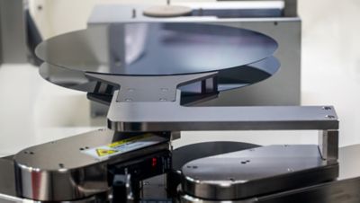
Integrate crack detection easily into existing systems
The CrackScan optical inspection system precisely detects and identifies tiny cracks inside a wafer. The high-speed line scan cameras reliably detect defects such as LLS, PID, or COP with the highest precision, even at maximum throughput rates.
The system is easy to integrate into existing fully automated production lines. CrackScan can be used either as a standalone system or combined in a cluster with other inspection processes like WafQScan and SpecGAGE3D. CrackScan can be supplemented with EdgeScan to detect defects like chippings and scratches on the wafer edge.
- Seamless integration into existing process lines
- Detection of natural and artificial micro cracks in high-speed
- Tailor-made optical setup allows significant increase in detection performance
- Flexible integration into high volume wafer handling systems, as well as existing system
- SEMI-compliant construction for clean room operation in FEOL
Download additional information
 CrackScan brochure en
CrackScan brochure en
- Filename
- brochure-crackscan-semiconductor-en.pdf
- Größe
- 311 KB
- Format

CrackScan brochure cn
- Filename
- brochure-crackscan-semiconductor-cn.pdf
- Größe
- 488 KB
- Format